Double Layer PCB With Black Solder Mask Immersion Gold
1 2 Layer FR4 substrate material printed circuit board.
2 ROHS, MSDS, SGS, UL, ISO9001&ISO14001 Certificated.
3 FR4 TG150 material, pcb thickness is 1.6mm.
4 Black solder mask and white silkscreen.
5 35um copper on each layer.
6 PCB size is 250mm*130mm/4pcs.
7 Surface treatment is immersion gold 1u'.
8 Customized pcb, need customer to send us the gerber file or pcb
file.
- S1150G Material Data Sheet:
| S1150G |
| Items | Method | Condition | Unit | Typical Value |
| Tg | IPC-TM-650 2.4.25 | DSC | ℃ | 155 |
| Td | IPC-TM-650 2.4.24.6 | 5% wt. loss | ℃ | 380 |
| CTE (Z-axis) | IPC-TM-650 2.4.24 | Before Tg | ppm/℃ | 36 |
| After Tg | ppm/℃ | 220 |
| 50-260℃ | % | 2.8 |
| T260 | IPC-TM-650 2.4.24.1 | TMA | min | >60 |
| T288 | IPC-TM-650 2.4.24.1 | TMA | min | 30 |
| Thermal Stress | IPC-TM-650 2.4.13.1 | 288℃, solder dip | -- | pass |
| Volume Resistivity | IPC-TM-650 2.5.17.1 | After moisture resistance | MΩ.cm | 6.4 x 10⁷ |
| E-24/125 | MΩ.cm | 5.3 x 10⁶ |
| Surface Resistivity | IPC-TM-650 2.5.17.1 | After moisture resistance | MΩ | 4.8 x 10⁷ |
| E-24/125 | MΩ | 2.8 x 10⁶ |
| Arc Resistance | IPC-TM-650 2.5.1 | D-48/50+D-4/23 | s | 140 |
| Dielectric Breakdown | IPC-TM-650 2.5.6 | D-48/50+D-4/23 | kV | 45+kV NB |
| Dissipation Constant (Dk) | IPC-TM-650 2.5.5.9 | 1MHz | -- | 4.8 |
| IEC 61189-2-721 | 10GHz | -- | — |
| Dissipation Factor (Df) | IPC-TM-650 2.5.5.9 | 1MHz | -- | 0.01 |
| IEC 61189-2-721 | 10GHz | -- | — |
| Peel Strength (1Oz HTE copper foil) | IPC-TM-650 2.4.8 | A | N/mm | — |
| After thermal Stress 288℃,10s | N/mm | 1.4 |
| 125℃ | N/mm | 1.3 |
| Flexural Strength | LW | IPC-TM-650 2.4.4 | A | MPa | 600 |
| CW | IPC-TM-650 2.4.4 | A | MPa | 450 |
| Water Absorption | IPC-TM-650 2.6.2.1 | E-1/105+D-24/23 | % | 0.1 |
| CTI | IEC60112 | A | Rating | PLC 0 |
| Flammability | UL94 | C-48/23/50 | Rating | V-0 |
| E-24/125 | Rating | V-0 |
Q1: What is High Potential (HiPot) Testing?
A1: The High Potential (HiPot) test is conducted to check whether the
dielectric material of a PCB board can withstand a voltage higher
than its rated voltage without breaking down. This is a type of
stress test helps measure the dielectric strength of the PCB
substrate which in turn helps to measure the insulation capability
of the Device Under Test (DUT). It also gives an idea to how much
voltage the DUT can withstand during real-life applications.
In this test, a high voltage is supplied to the PCB board for a few
seconds to check for the insulation or dielectric strength of the
components mounted on the PCB board. The duration of the HoPot test
can vary from a few seconds to up to a few minuets. The IEC 60950
standard says the test must be conducted for 1 minute. A board is
subjected to the HiPot test only after conducting fault detection,
humidity, and vibration tests.
Both AC and DC can be used to carry out HiPot Test. This can depend
on the requirements established by the regulatory testing agency.
However it is best to test an AC Powered device with a high AC
Voltage and a DC powered device with a high DC voltage.
How to calculate HiPot test voltage?
There is no exact way to calculate the HiPot voltage, however a
general rule of thumb would be (2 x Nominal input voltage) + 1000
V. For an instance, if the operating input voltage is 140 Volts
then the HiPot Voltage would be (140 x 2) V + 1000 V = 1280 V or
1.28 KV.
How is a HiPot Test performed?
This test can be performed by applying a high voltage to the
Printed Circuit Board or Device in which the PCB is used and
monitoring the resulting leakage current. The voltage that is
applied in a HiPot Test can be up to 10 times higher than the rated
voltage of the PCB. The voltage is applied between the main input
and the chassis (outer framework) of the product.

In the above figure, we have considered a basic circuit to
demonstrate the condition of HiPot test
HiPot Test Pass Condition:
If the substrate of the PCB can resist the high voltage without
breaking down and also inhibits the flow of leakage current then it
can be seen as a HiPot pass condition.

Good insulation will not allow the flow of excess leakage current
on the surface of the device.
HiPot Test Fail Condition:
If the breakdown occurs and there is no control on the leakage
current then it can be considered as a HiPot fail condition.
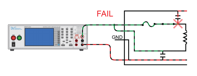
Poor insulation can cause the flow of excess leakage current on the
surface of the device under test.


