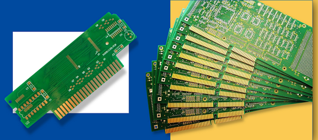
Gold Finger PCB 4 Layer Printed Circuit Board 1.6 MM Thickness
1 4 Layer printed circuit board with gold fingers.
2 Gold thickness is 30U' on gold fingers.
3 FR4 sustrate material, tg170 degree.
4 Gold plating on gold fingers, for balance pads, we do immersion
gold treatment.
5 1OZ finished cooper thickness on each layer.
6 Min line space and width is 5/5mil.
7 Drawing size is 270mm*185mm/1pcs.
8 ROHS, MSDS, SGS, UL, ISO9001&ISO14001 Certificated.
- Our production applications:
1 Consumer electronic products: SSD, TWS earphones,
headsets,computer devices, portable power supplies, bluetooth
modules, gps modules, wifi modules, smart keys for cars,
intelligent locks, floor mopping robots, zigbee, etc.
2 Industrial control:main boards in machines, industrial robots,
servo motors etc.
3 Automotive: BMS main boards, automotive radar etc.
4 Power supplies: UPS, industrial power supply, frequency power
supply.
5 Medical: medical equipment, medical equipment power supply.
6 Communication products: 5G base station, routers, satellites,
antennas.
Q1: What are PCB Gold Fingers?
A1:
Gold Fingers are the gold plated narrow connectors found on the
edge of printed circuit boards to enable connections between
multiple boards. They are made from flesh gold, the hardest form of
gold available and work for a long time with superior conductivity.
The thickness of gold fingers usually ranges from 3 to 50 microns.
Gold is chosen for these fingers as it has the highest corrosion
resistance and electrical conductivity after Copper and Silver.
Sometimes, Gold is combined with Cobalt and Nickel to increase the
resistance of the fingers for wear and tear. PCBs are
connected/disconnected from each other multiple times. So these
connection points (fingers) need to be able to handle some wear and
tear.
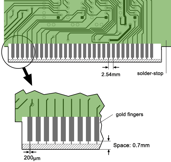
What is PCB Gold Finger Beveling?
The PCB Gold Fingers plating process starts after the solder mask
deposition and before the surface finish. It includes the following
steps:
- Nickel Plating: Initially, between 2 to 6 microns of Nickel is
plated to the connector edges of the fingers.
- Gold Plating: In this step, between 1 to 2 microns of hard Gold is
plated over the Nickel layer. In general practice, Cobalt is also
added to Gold to boost the surface resistance.
- Beveling: The edges are then beveled/ tapered at a particular angle
(30 to 45 degree) to make easier insertion to the corresponding
slot

Design Specifications for PCB Gold Fingers:
- The inner PCB layers towards the PCB edges must be Copper-free, to
prevent exposure at the time of Beveling.
- It is not advisable to include the plated through holes (PTH)
within 1 mm of Gold Fingers.
- Maintain at least 0.5 mm of distance between the gold fingers and
the board outline.
- Any compromise with the standard spacing values can lead to weak
and malfunctioned PCB board.
- No soldermask or screen printing should be performed near the Gold
Fingers.
- The Gold Fingers should be placed facing outwards from the PCB’s
center.
PCBs with Non-uniform Gold Fingers:
For some PCBs, the gold fingers are intended to be shorter than
others. The most relevant example of such PCB is the one used for
memory card readers, where the device linked with long fingers must
be powered first to those connected with the shorter fingers.
PCBs with Segmented Gold Fingers
Segmented gold fingers vary in length and some of them are also
disjoined within the same fingers of the same PCB. Such PCBs are
suitable for water-resistant and rugged electronics.

Quality Measures for PCB Gold Fingers:
The Association Connecting Electronics Industries (IPC) has
prescribed some standards for the production of PCB Gold Fingers.
The IPC standards are summarized as follows:
- Chemical composition: To achieve maximum rigidity along the edges
of PCB Gold Fingers, the gold plating should consist of between 5
to 10% Cobalt.
- Thickness: The plating thickness should be in the range of 2 to 50
microinches. The standard thicknesses by size are 0.031 inches,
0.062 inches, 0.093 inches, and 0.125 inches.
- Visual test: The visual inspection is performed through a
magnifying lens. The contact edges should be smooth, have a clean
surface and also be free from excess plating like Nickel.
- Tape test: It is conducted to check the adhesiveness of the gold
plating along the contacts. In this test, a strip of tape is
fastened over the contact edges followed by removing the same. In
the next step, the tape is inspected for traces of plating. If any
gold is visible on the tape, then the plating is considered as
insufficient for continuous injection and ejection.


