| Sign In | Join Free | My himfr.com |
|
| Sign In | Join Free | My himfr.com |
|
| Ask Lasest Price | |
| Brand Name : | WITGAIN PCB |
| Model Number : | HDIPCB0009 |
| Certification : | UL |
| Price : | negotiable |
| Payment Terms : | T/T |
| Supply Ability : | 100k pcs/month |
| Delivery Time : | 20 days |
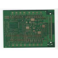
HDI PCB High Density Interconnected Printed Circuit Board With Blind And Buried Holes
1 10 Layer HDI PCB, high density printed circuit board.
2 Bline holes: L1-L2 0.1MM, L2-L3 0.1MM, L9-L10 0.1MM, L8-L9 0.1MM
3 Buried holes: L4-L7 0.2MM.
4 Via holes: L1-L10 0.2MM.
5 PCB thickness is 1.0mm.
6 Min BGA ball size is 8mil.
7 Min line space and width is 3/3mil.
8 Material is FR4 Substrate, tg180 degree
9 S1000-2 material used.
| S1000-2 | |||||
| Items | Method | Condition | Unit | Typical Value | |
| Tg | IPC-TM-650 2.4.25 | DSC | ℃ | 180 | |
| IPC-TM-650 2.4.24.4 | DMA | ℃ | 185 | ||
| Td | IPC-TM-650 2.4.24.6 | 5% wt. loss | ℃ | 345 | |
| CTE (Z-axis) | IPC-TM-650 2.4.24 | Before Tg | ppm/℃ | 45 | |
| After Tg | ppm/℃ | 220 | |||
| 50-260℃ | % | 2.8 | |||
| T260 | IPC-TM-650 2.4.24.1 | TMA | min | 60 | |
| T288 | IPC-TM-650 2.4.24.1 | TMA | min | 20 | |
| T300 | IPC-TM-650 2.4.24.1 | TMA | min | 5 | |
| Thermal Stress | IPC-TM-650 2.4.13.1 | 288℃, solder dip | -- | 100S No Delamination | |
| Volume Resistivity | IPC-TM-650 2.5.17.1 | After moisture resistance | MΩ.cm | 2.2 x 10⁸ | |
| E-24/125 | MΩ.cm | 4.5 x 10⁶ | |||
| Surface Resistivity | IPC-TM-650 2.5.17.1 | After moisture resistance | MΩ | 7.9 x 10⁷ | |
| E-24/125 | MΩ | 1.7 x 10⁶ | |||
| Arc Resistance | IPC-TM-650 2.5.1 | D-48/50+D-4/23 | s | 100 | |
| Dielectric Breakdown | IPC-TM-650 2.5.6 | D-48/50+D-4/23 | kV | 63 | |
| Dissipation Constant (Dk) | IPC-TM-650 2.5.5.9 | 1MHz | -- | 4.8 | |
| IEC 61189-2-721 | 10GHz | -- | — | ||
| Dissipation Factor (Df) | IPC-TM-650 2.5.5.9 | 1MHz | -- | 0.013 | |
| IEC 61189-2-721 | 10GHz | -- | — | ||
| Peel Strength (1Oz HTE copper foil) | IPC-TM-650 2.4.8 | A | N/mm | — | |
| After thermal Stress 288℃,10s | N/mm | 1.38 | |||
| 125℃ | N/mm | 1.07 | |||
| Flexural Strength | LW | IPC-TM-650 2.4.4 | A | MPa | 562 |
| CW | IPC-TM-650 2.4.4 | A | MPa | 518 | |
| Water Absorption | IPC-TM-650 2.6.2.1 | E-1/105+D-24/23 | % | 0.1 | |
| CTI | IEC60112 | A | Rating | PLC 3 | |
| Flammability | UL94 | C-48/23/50 | Rating | V-0 | |
| E-24/125 | Rating | V-0 | |||
Q1: What is HDI PCB?
A1: HDI is the abbreviation of high density interconnector. Generally, there are blind and buried holes in HDI PCB. Due to the space limits, some product need to very small size pcb. HDI pcb was generated to save space and increase interconnectors.

|


