| Sign In | Join Free | My himfr.com |
|
| Sign In | Join Free | My himfr.com |
|
| Ask Lasest Price | |
| Brand Name : | WITGAIN PCB |
| Model Number : | HDIPCB0011 |
| Certification : | UL |
| Price : | negotiable |
| Payment Terms : | T/T |
| Supply Ability : | 100kpcs/Month |
| Delivery Time : | 25 days |
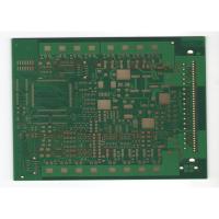
Selective Immersion Gold 6 Layer HDI PCB With Blind Holes And Buried Holes
PCB Specifications:
1 Part NO: HDIPCB0011
2 Layer Count: 6 Layer HDI PCB
3 Finished Board Thickness: 1.0MM
4 Drilling: L1-L2 0.1MM, L2-L5 0.2MM, L5-L6 0.1MM, L1-L6 0.2MM
5 Min Lind Space&Width: 2.8/2.7mil
6 Copper Thickness: 1/H/H/H/H1
7 Application Area: Smart Watch
8 PCB Size: 113.1MM*101.1MM/6PCS
Our production applications:
1 Consumer electronic products: SSD, TWS earphones, headsets,computer devices, portable power supplies, bluetooth modules, gps modules, wifi modules, smart keys for cars, intelligent locks, floor mopping robots, zigbee, etc.
2 Industrial control:main boards in machines, industrial robots, servo motors etc.
3 Automotive: BMS main boards, automotive radar etc.
4 Power supplies: UPS, industrial power supply, frequency power supply.
5 Medical: medical equipment, medical equipment power supply.
6 Communication products: 5G base station, routers, satellites, antennas.
IT180A DATA SHEET:
| Items | IPC TM-650 | Typical Value | Unit |
| Peel Strength, minimum A. Low profile copper foil B. Standard profile copper foil | 2.4.8 | 5 8 | lb/inch |
| Volume Resistivity | 2.5.17.1 | 1x10⁹ | M-cm |
| Surface Resistivity | 2.5.17.1 | 1x10⁸ | M |
| Moisture Absorption, maximum | 2.6.2.1 | 0.10 | % |
| Permittivity (Dk, 50% resin content) A. 1MHz B. 1GHz | 2.5.5.9 2.5.5.9 | 4.5 4.4 | -- |
| Loss Tangent (Df, 50% resin content) A. 1MHz B. 1GHz | 2.5.5.9 2.5.5.9 | 0.014 0.015 | -- |
| Flexural Strength, minimum A. Length direction B. Cross direction | 2.4.4 | 500-530 410-440 | N/mm2 |
| Thermal Stress 10 s at 288°C A. Unetched B. Etched | 2.4.13.1 | Pass Pass | Rating |
| Flammability | UL94 | V-0 | Rating |
| Comparative Tracking Index (CTI) | IEC 60112 / UL 746 | CTI 3 (175-249) | Class (Volts) |
| Glass Transition Temperature(DSC) | 2.4.25 | 175 | ˚C |
| Decomposition Temperature | 2.4.24.6 | 345 | ˚C |
| X/Y Axis CTE (40℃ to 125℃) | 2.4.41 | 11-13 / 13-15 | ppm/˚C |
| Z-Axis CTE A. Alpha 1 B. Alpha 2 C. 50 to 260 Degrees C | 2.4.24 | 45 210 2.7 | ppm/˚C ppm/˚C % |
| Thermal Resistance A. T260 B. T288 | 2.4.24.1 | >60 20 | Minutes Minutes |
A1: Thermal Resistance is a property of a printed circuit board that specifies its resistance to heat dispersion. A low thermal resistance in a PCB makes the dispersion of heat easier. This is basically the inverse of thermal conductivity. The thermal resistance of a PCB can be calculated by evaluating all the layers of the board and the heat parameters of the material.
To find the total thermal resistance for your board, you must include all layers of the board and the associated heat parameters for the type of material through which heat will flow.
[Formula]
R_theta = absolute thermal resistance (K/W) across the thickness of the sample
Delta x = thickness (m) of the sample (measured on a path parallel to the heat flow)
k = thermal conductivity (W/(K·m)) of the sample
A = cross-sectional area (m2) perpendicular to the path of heat flow
In addition to the thermal resistance of the board. The Thermal resistance of Vias must also be calculated. This usually depends on the copper trance, the laminate and the substrate and their respective thermal resistivities.
How can you reduce the Thermal Resistance of a PCB?

|


