Special Features: big size, Gold Finger with ENIG 1u' and solder
mask ink plugged via hole
Standard: IPC-A-600G Class II Certificates: UL/94V-0/ISO
Our Product Categories:
Our Product Categories
Material Kinds
Layer Counts
Treatments
FR4
Single Layer
HASL Lead Free
CEM-1
2 Layer/Double Layer
OSP
CEM-3
4 Layer
Immersion Gold/ENIG
Aluminum Substrate
6 Layer
Hard Gold Plating
Iron Substrate
8 Layer
Immersion Silver
PTFE
10 Layer
Immersion Tin
PI Polymide
12 Layer
Gold fingers
AL2O3 Ceramic Substrate
14 Layer
Heavy copper up to 8OZ
Rogers, Isola high frequency materials
16 Layer
Half plating holes
Halogen free
18 Layer
HDI Laser drilling
Copper based
20 Layer
Selective immersion gold
22 Layer
immersion gold +OSP
24 Layer
Resin filled in vias
FAQ:
Q:Via hole plugging – what is it and when can it be used
A:
Via hole plugging is a PCB manufacturing technique in which the via
hole is filled with solder mask or epoxy. This process partially or
completely closes the via hole using a conductive or non-conductive
filling material. Filling via holes results in more reliable
surface mounts, provide better assembly yields and improve
reliability of the PCB by decreasing the probability of trapped air
or liquids in the via and thus the PCB Board.
Are there different types of via hole plugging or protection? Are
there variants when calling for a ‘plugged’ via? Yes there are. In
fact there are seven types of via hole ‘protection’. Some are
recommended and some are not, some are necessary for certain
technologies, and all have different ‘names’. In this text, we will
explain some of them.
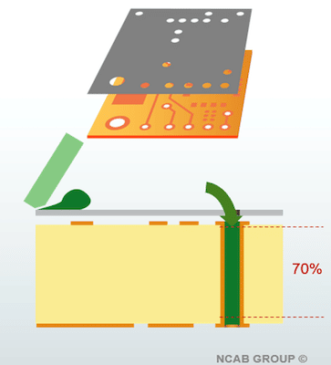
What is a via?
A via is a plated through hole (PTH) in a PCB that is used to
provide electrical connection between a trace on one layer of the
printed circuit board to a trace on another layer. Since it is not
used to mount component leads, it is generally a small hole and pad
diameter. The following are the two processes that can achieve
this.
No 1: Soldermask covered (Tented)
A via tenting is nothing more than covering its annular copper ring
with solder resist, also known as LPI (Liquid Photo Imageable) ink.
PCB designers need to remove the solder mask opening from its via
in their design, which enables via tenting. This is why it’s
considered standard and won’t increase the price of the PCB. In
this process, we can only ensure that the annular copper ring is
covered with solder resist ink. The surface of the hole may or may
not be covered with the solder resist ink.
It is very important to note that the smaller the via hole size,
the better the result will be. Suggested is a via >=0.20mm. Via
hole sizes less than 0.3mm have the best chance of getting filled,
while between 0.3mm to 0.5mm sizes, filling results may vary.
Because this is an uncontrolled process, it is not recommended when
holes need to be closed. Advantages:
No cost involved because via filling is achieved during the
standard PCB process (screen printing process costs extra).
See Table 1 for the main benefits, degree of certainty and cost
drivers.
Disadvantages:
Not suitable if a design demands 100% guaranteed filled via.
Not suitable for Via In Pad process (for active via) and therefore
not recommended for highly-complex designs having a fine pitch BGA.
No 2: Soldermask plug
Compared to tented vias, via holes are also filled with solder
resist ink (LPI) in this process.
Screen printing process
In this process, a drilled ALU sheet is used to push standard
solder resist ink (LPI) into the via holes that need to be filled.
The normal solder mask process is carried out after this screen
printing process. 100% guaranteed result is assured in this
process. Advantages:
Less expensive in cost compared to via plugging (conductive or
non-conductive) process.
This makes it ideal if it’s just about filling vias with 100%
certainty.
See Table 1 for the main benefits, degree of certainty and cost
drivers.
Disadvantages:
Not suitable for Via In Pad process (i.e. for active via)
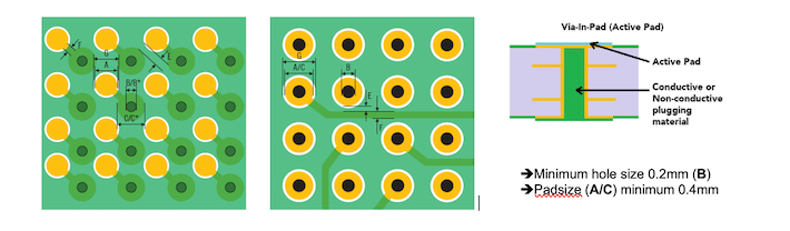
Via Plugging (Via In Pad – conductive or non-conductive)
To manufacture products that are more and more compact and
advanced, electronic engineers are facing a challenge to design
circuit boards that are smaller without compromising performance.
Therefore, BGA packages with smaller pitch or clearances are
becoming more popular. Instead of using the standard “dog bone”
footprint, where signals are transferred from the BGA pad to a via
and then from the via to other layers, the via can be drilled
directly into the BGA pad. This makes the routing of track work
tighter and easier in designing PCBs as the surface of via itself
becomes BGA pad allowing it to be treated as a normal SMD pad for
soldering. This process is called “Via In Pad” while the pad is
called an “Active Pad”.
Overall, there are two types of via plugging available depending on
the material used in plugging process; non-conductive via plugging
and conductive via plugging. Out of these two, the most common and
widely preferable is non-conductive via plugging.
Conductive Via Plugging
For PCB designs that require to transfer high amount of heat or
current from one side of the board to another, conductive via
plugging is a handy solution. It can also be used to dissipate
excessive heat generated underneath some components. The metallic
nature of the fill will naturally wick heat away from the chip to
the other side of the board in many ways like a radiator.
Advantages:
Heat sink or transfer where other conventional methods are
impractical e.g. underneath the chip component.
Increased current carrying capacity due to higher thermal
conductivity (between 3.5 to 15 W/mK) of the conductive material.
Disadvantages:
High instability of copper pad and copper plating inside the via
hole barrel. This occurs due to the difference in CTE (coefficient
of thermal expansion) value of conductive material and laminate
surrounding it. When the PCB goes through thermal cycles, metal
will heat and expand more rapidly than surrounding laminate, which
can cause a fracture between pad and via hole barrel and lead to an
open circuit
Thermal conductivity is not too high (compared to electroplated
copper that has thermal conductivity of more than 250W/mK) so it is
possible to add a few more vias and avoid this process to more
reliable non-conductive via plugging
More expensive than non-conductive via plugging
Not in high demand so minimal manufacturers can supply
Non-Conductive Via Plugging or Epoxy Resin Plugging
This is the most common and popular method of via plugging,
especially for Via In Pad process. The barrel of via hole is filled
with non-conductive material. Selection of the material depends on
the CTE value, availability, specific design requirements and type
of plugging machine. Thermal conductivity of non-conductive
material is normally close to 0.25 W/mK. A common misconception
about non-conductive via plugging is that the via will either not
pass any current or only a weak electrical signal, which is
absolutely not correct. The via will still be plated as normal
before non-conductive material is plugged inside. It means via will
work as normal as in any other standard PCB.
Advantages:
Prevents solder or any other contaminants from entering into via
Provides strength and structural support to active pads (Via In Pad
process)
Offers better stability and reliability of pad and via due to close
match of CTE between filling material and surrounding laminate when
comparing the same with conductive material
Witgain Technology Limited was established in 2007. Factories
locate in HuiZhou City and marketing locates in ShenZhen City. The
total area of two factories is around 10000 square meters. We can
offer 2-layer and multi-layer pcb services to our customers,
highest to 24 layers and rigid-flex pcb, ceramic pcb, HDI pcb,
heavy copper pcb are also included. To meet our customer's
diversified demands, we also accept prototype orders, small batch
orders and big batch orders. Quality and technology is what we
value most and we will never stop improving our capabilities. Our
customers' satisfaction is always what we are seeking for.